To achieve highly efficient and bright thin-film LEDs, a combination of factors is necessary for the light-emitting materials. These include high PLQE, high charge mobilities and low quantum efficiency droop. Traditional thin-film LEDs, such as organic LEDs, face challenges in achieving high efficiency at high brightness owing to their low charge mobility and susceptibility to Auger or excitonic quenching7. In recent studies, it has been demonstrated that low-dimensional perovskites with multiple-quantum-well or quantum dot structures, making use of quantum confinement effects, can effectively suppress nonradiative recombination8,9,10. This phenomenon allows them to achieve near 100% PLQE9. However, these low-dimensional perovskite materials often exhibit low charge mobility and suffer from severe Auger recombination, which limits their potential for efficient LEDs at high brightness8,11. On the other hand, 3D perovskites have emerged as promising materials for the development of efficient and bright thin-film LEDs. They have high charge mobility and show low quantum efficiency droop. Furthermore, 3D perovskites can naturally form discrete, sub-micrometre-scale structures, leading to an enhanced light outcoupling efficiency greater than 30% (ref. 1). Recent advancements have showcased large-sized, flexible, efficient and bright LEDs based on discrete 3D perovskites with excellent stability12. However, one challenge faced by 3D perovskites is their slow radiative recombination rate, making their PLQE highly susceptible to defects4,13. To address this issue, various passivation strategies have been used to reduce the defect density in 3D perovskite films, approaching levels comparable with single crystals3. Despite substantial efforts, the maximum achievable PLQE only reaches approximately 80%, with resulting LEDs exhibiting peak EQEs of less than 25% (refs. 3,4).
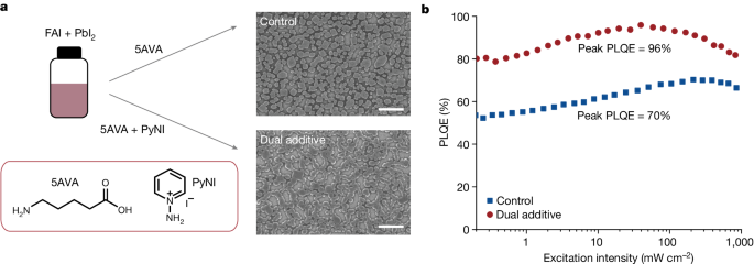
Here we demonstrate efficient, near-infrared 3D perovskites by accelerating the radiative recombination through formation of tetragonal FAPbI3 perovskite using a dual-additive method. The fabrication process is shown in Fig. 1a. A precursor solution was prepared using 1-aminopyridinium iodide (PyNI), 5-aminovaleric acid (5AVA), formamidinium iodide (FAI) and PbI2 with a molar ratio of 0.15/0.25/2.40/1.00 dissolved in N,N-dimethylformamide (DMF; 8.5 wt%) (see Methods for details), in which PyNI and 5AVA are both additives. For comparison, a control sample using only a single additive (5AVA) was also prepared1. We note that the role of 5AVA has been investigated previously, which can markedly enhance the LED efficiency by facilitating the formation of low-defect-density FAPbI3 perovskite with sub-micron discrete structures1. The control and dual-additive perovskites exhibit similar dispersed sub-micron grain morphologies (Fig. 1a and Extended Data Fig. 1), which can contribute to a light outcoupling efficiency greater than 30% in LED device architectures1 (Supplementary Note 1). Notably, the dual-additive sample shows a much higher PLQE of 96% compared with the control sample (about 70%) (Fig. 1b).
a, Fabrication of perovskite films and SEM images of control perovskite (with 5AVA) and dual-additive perovskite (with 5AVA and PyNI). Scale bars, 1 µm. Chemical structures of 5AVA and PyNI. b, Excitation-intensity-dependent PLQEs of control and dual-additive perovskites. Peak PLQEs are about 70% and about 96% for control and dual-additive perovskites, respectively.
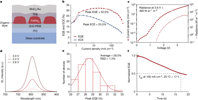
Then we fabricated and characterized LEDs based on the two samples mentioned above. The device structure was indium tin oxide (ITO)/polyethylenimine ethoxylated (PEIE)-modified zinc oxide (ZnO; 30 nm)/perovskite (approximately 60 nm)/poly(9,9-dioctyl-fluorene-co-N-(4-butylphenyl)diphenylamine) (TFB; 20 nm)/molybdenum oxide (MoOx; 5 nm)/gold (Au; 80 nm)1,3 (Fig. 2a and Extended Data Fig. 2a). The dual-additive perovskite LEDs exhibit a peak EQE as high as 32.0% at a current density of 20 mA cm−2, accompanied by a maximum brightness of 390 W sr−1 m−2 at a low voltage of 3.6 V (Fig. 2b,c). The EQE remains high, with a value of 30% at a high current density of 100 mA cm−2. The peak energy conversion efficiency (ECE) reaches 25.5% at a current density of roughly 1 mA cm−2 and is maintained at 16.0% at a high current density of 100 mA cm−2 (Supplementary Note 2). The electroluminescence (EL) peak is located at 805 nm (Fig. 2d), which is slightly redshifted compared with the control device (801 nm) (Extended Data Fig. 3c). The devices demonstrate good reproducibility, with an EQE histogram for 70 devices showing an average peak EQE of 28.5% (Fig. 2e). By contrast, the control device exhibits a peak EQE of approximately 20% (Extended Data Fig. 3a). Considering they have similar light outcoupling efficiency (Supplementary Note 1), we believe that the improved performance of the dual-additive device can be mainly attributed to its higher PLQE (Fig. 1b). Also, we conducted measurement on the half-life (T50) stability of our devices under a constant current density of 100 mA cm−2. The T50 lifetimes of the devices were found to be comparable, with the control sample lasting for 19 h (Extended Data Fig. 3d), which aligns closely with the reported result1, and the dual-additive device lasting for 17 h (Fig. 2f). We believe that the slightly shorter lifetime of the dual-additive device could be because of the slightly more excess iodide ions with the dual-additive perovskite film, as the ion migration is the main cause of the device degradation14.
a, Schematic of the device structure. b, Current-density-dependent EQE and ECE. The dual-additive perovskite LED can achieve a peak EQE of 32% under a current density of 20 mA cm−2. c, Dependence of current density and radiance on bias voltage. The maximum radiance is 390 W sr−1 m−2 at 3.6 V. d, EL spectra at various voltages. e, Histogram of peak EQEs. Statistics from 70 devices show an average peak EQE of 28.5%, with a relative standard deviation (RSD) of 1.4%. f, Stability of the device measured at a constant current density of 100 mA cm−2 at 20 °C. a.u., arbitrary units.
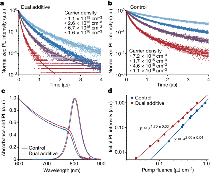
To verify why the dual-additive perovskite exhibits enhanced PLQE, we conducted time-resolved photoluminescence (TRPL) measurements under various excitation intensities. At an extremely low excitation intensity (with an initial carrier density of about 1013 cm−3), the TRPL of both the dual-additive perovskite and the control sample exhibit similar decay behaviour, indicating comparable trap densities between them15 (Extended Data Fig. 4). As the excitation intensities increase, the dual-additive perovskite exhibits accelerated photoluminescence (PL) decay compared with the control sample (Fig. 3a,b), which can be because of enhanced radiative recombination. To quantify this observation, we determined the first-order (trap-assisted and excitonic, k1) and second-order (bimolecular, k2) recombination rate constants for both samples by fitting the transient PL data, while keeping the third-order Auger recombination rate constant (k3)4 (Supplementary Note 3). The fitting results indicate that, regardless of the injected carrier density, the k2 value of the dual-additive perovskite surpasses that of the control sample by several folds, and k1 is approximately one order of magnitude higher for the dual-additive perovskite compared with the control sample (Extended Data Table 1). We found negligible effects on the fitting results by increasing/decreasing k3 for one order of magnitude (Supplementary Note 3). Because the trap densities between them are similar, the enhanced k1 in dual-additive perovskite is mainly because of the enhancement of excitonic (radiative) recombination instead of trap-assisted (nonradiative) recombination, which is consistent with the high PLQE observed in Fig. 1b under low excitation intensities. On the basis of these findings, we can conclude that the enhanced PLQE of the dual-additive perovskite film is associated with increased radiative recombination rates (both excitonic and bimolecular), rather than a decreased nonradiative recombination rate typically observed through defects passivation in previous studies1,2,3.
TRPL (scatter plots) under various excitation intensities and fitted by dynamics of charge-carrier models (curves) for dual-additive perovskite film (a) and control sample (b). c, Absorption and steady PL spectra of control and dual-additive perovskites. d, Logarithm plot of the integrated initial PL intensity (IPL[t = 0]) versus excitation density. a.u., arbitrary units.
We then investigate the underlying mechanism behind the enhanced radiative recombination rates. We observe that the absorption edge of the dual-additive perovskite film become more obvious (Fig. 3c), indicating a stronger excitonic feature compared with the control sample. By fitting the absorption spectra near the band edge based on Elliott’s theory16 (Supplementary Note 4), we obtain an exciton binding energy (Eb) of 13.9 meV for the dual-additive perovskite film, which is much higher than that of the control sample (3.9 meV) (Extended Data Fig. 5). The increased Eb can lead to higher population of excitons in the excited states and enhance radiative recombination17,18, which is consistent with the fitting results (Extended Data Table 1). The more excitonic recombination can be further confirmed by power-dependent TRPL measurements at the zero time (IPL[t = 0]) (Fig. 3d). In these experiments, the PL intensities were measured immediately after the ultra-fast (fs) excitation, which can precisely determine the carrier-density-dependent PL intensity13. We then fit the PL intensities using a power-law function of the form PL ≈ Pk, in which P represents excitation fluence and k is a real-number exponent providing information on the order of recombination. For dual-additive perovskite, a k value of 1.7 indicates the coexistence of free carriers (bimolecular recombination) and excitons (monomolecular recombination) (Supplementary Note 5). Conversely, IPL[t = 0] of the control perovskite increases quadratically (meaning a k value of 2) with the excitation fluence, suggesting predominantly bimolecular recombination. Therefore, we believe that the accelerated radiative recombination of the dual-additive perovskite is because of the increased Eb, which is consistent with previous studies on the 3D FAPbI3 perovskite at low temperatures19.
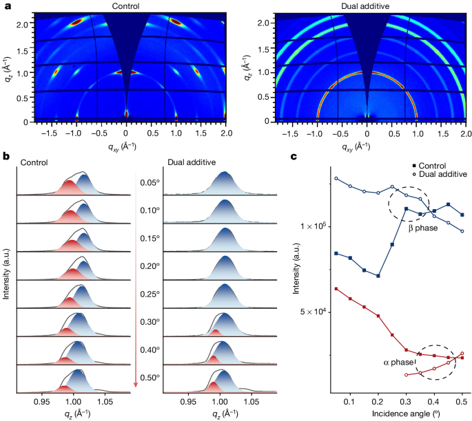
The enhanced exciton binding energy in perovskites can result from increased space confinement of crystal grains or phase transitions19,20,21. In both the EL and PL spectra of the dual-additive perovskite, we observe an approximately 4 nm redshift compared with those of control sample (Figs. 2d and 3c and Extended Data Fig. 3c). This indicates that the dual-additive perovskite does not have enhanced space confinement. Otherwise, one would anticipate a blueshift in the emission. So, we can infer that a phase transition is responsible for the observed increase in binding energy. Also, because the dual-additive perovskite shows a similar trap density to the control sample, we believe that the trap-induced redshift does not occur in this case22. To investigate the crystal structure of the perovskite films, we conducted grazing-incidence wide-angle X-ray scattering (GIWAXS) analysis, varying the incidence angles (0.05° to 0.50°) to examine both the surface and bulk regions of the films. As shown in Fig. 4a, both the dual-additive perovskite and the control sample exhibit characteristic scattering at q ≈ 1.00 Å−1, which is attributed to the cubic or tetragonal perovskite23,24. Notably, the control sample shows the overlapping of discrete Bragg scattering spots and scattering rings (or arcs), whereas the dual-additive perovskite shows a scattering ring isotropic in polar angle. This result suggests a preferential stacking of vertical-oriented octahedrons along the surface-normal direction in the control sample, along with a small amount of random crystalline orientation (Extended Data Fig. 6), whereas the dual-additive perovskite has a random crystalline orientation (Extended Data Fig. 7). This observation is consistent with our morphology characterization that shows several types of grain packed in the dual-additive film (Extended Data Fig. 2b). We then analysed the qz direction of 1D GIWAXS at various probing angles (or depths) (Fig. 4b). It shows that the control sample exhibits a uniform distribution of both cubic and tetragonal phases throughout the film. By contrast, the upper part of the dual-additive film is predominantly composed of a single tetragonal phase (0.05° to 0.25°), whereas the lower part exhibits mainly tetragonal phase with a small amount of cubic phases (Fig. 4c). It is consistent with the observed redshifted EL and PL spectra of the dual-additive perovskite film, as the tetragonal phase of FAPbI3 (refs. 19,25). On the basis of these investigations, we can conclude that the increased exciton binding energy in the dual-additive film is primarily attributed to the higher proportion of the tetragonal phase, which is consistent with the observation of the perovskite under low-temperature conditions19,25. Also, our transient PL measurement further shows that there is no substantial energy transfer occurring between the two phases (Supplementary Fig. 4), probably because of their very close bandgaps25 (Supplementary Note 6). Moreover, because the ZnO electron transport layer has a much higher charge mobility than the TFB hole transport layer26,27, we can expect that the electron–hole recombination mainly occurs near the interface of perovskite and TFB, which is predominantly of single tetragonal phase.
a, 2D GIWAXS patterns of control and dual-additive perovskite films with the incidence angle of 0.20°. b, 1D GIWAXS patterns along qz with various incidence angles. GIWAXS probing depth was varied by changing the angle of incidence of the X-ray beam from 0.05° to 0.50° (arrow indicates the incidence angles). Lower incidence angles imply a smaller probing depth in the perovskite surface, whereas larger angles indicate the detection of bulk perovskite. Owing to the distinct lattice spacings (d) between the cubic and tetragonal phases, measuring 6.40–6.35 Å and 6.34–6.30 Å, respectively, subtle variations in their corresponding q values were obtained24. The cubic phase (red) demonstrates a slightly smaller q value compared with the tetragonal phase (blue). c, Scattering intensity (peak area) obtained from the qz fitting with various incidence angles. a.u., arbitrary units.
To investigate how the dual additives can induce an increased proportion of the tetragonal phase, we conducted in situ absorption-spectra measurements during the film-annealing process (Extended Data Fig. 8). We observe that PyNI-additive-alone perovskite film exhibits dominant absorption peaks at 445 nm (PbI42−) and 490 nm (PbI64−), similar to the samples without additive or with 5AVA alone28. Notably, the PyNI-additive-alone and dual-additive films show a rapid decrease in absorption at 445 nm, along with an increase at 490 nm, indicating that PyNI can facilitate the conversion of PbI42− to PbI64− during annealing. In the cases of the 5AVA-alone and dual-additive films, we observe a further absorption peak at 545 nm, which can be attributed to the formation of a 5AVA-related low-dimensional intermediate phase3. These results indicate the coexistence of two crystallization pathways in the dual-additive system induced by the two additives separately. Previous studies have shown that the competition between these two crystallization pathways can lead to the confinement of the crystals, resulting in a higher proportion of the tetragonal phase29,30. Notably, from scanning transmission electron microscopy (STEM) measurements, we can observe the variation in Kikuchi line patterns among various regions within each particle for the dual-additive perovskite (Extended Data Fig. 2b). This suggests that the particles in dual-additive perovskite consist of several grains that are tightly connected or interlocked. We believe that our result of the formation of more tetragonal phase in dual-additive perovskite is consistent with previous studies.
To achieve high-efficiency LEDs with superior brightness, it is crucial to use light-emitting materials that exhibit high PLQEs, minimal Auger or excitonic quenching, high charge mobilities and preferably have structures conducive to efficient light outcoupling. Existing thin-film light-emitting materials, including organic semiconductors, quantum dots and low-dimensional perovskites, have fallen short of meeting all these criteria simultaneously. In our study, we present a straightforward approach to address this challenge by using 3D perovskites with increased exciton binding energy, which facilitate an accelerated rate of radiative recombination. By promoting the formation of tetragonal FAPbI3 perovskite, we have successfully achieved a near-unity PLQE in the 3D perovskite film. This remarkable achievement has enabled us to realize LEDs with an unprecedented EQE record of 32.0%. Our work holds pivotal importance in paving the way for continuous advancements in breaking the efficiency limits of perovskite LEDs and unlocks their full capabilities in next-generation display and lighting technologies.


